News
- PCB multilayer board stacking planning method
Source: Yaheng PCB Co., Ltd Time: 2023-07-22 Views: 679
-
Many PCB designers in the design of multilayer boards may not be very good at opening the brain to plan an efficient line layout, but always speculative, simply stacking layers on the board.
The disadvantages of stacking layers on the board are obvious. First of all, the simple stacking of layers will make the structure of the PCB circuit board becomes extremely complex and less reliable. Furthermore, the more layers, the more complex the production process, the higher the production costs, the more expensive the circuit board.
Obviously, we should start the design of multilayer PCB circuit boards when the board stack planning, including but not limited to the production and manufacturing of PCB used in the substrate and transmission parameters, but also consider impedance discontinuity, signal coupling, unintentional formation of the return path, high AC impedance and excessive electromagnetic radiation and other issues.
For the design of high-speed laminated circuit boards, Tontek Circuit gurus to everyone's advice is:
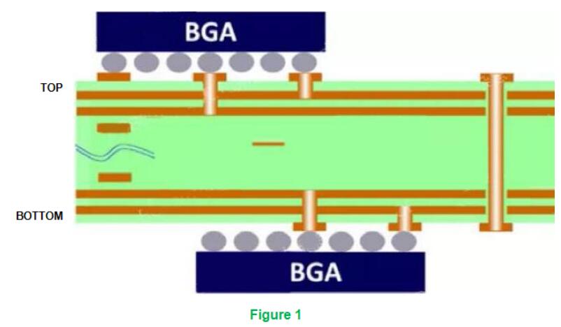
1. Couple the GND/PWR surface closely on layers 2 and 3, and on layers 2 and 3 counting from the bottom to the top (Figure 1). This will reduce the AC impedance of the PDN and provide low inductive power to the device.

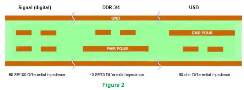
2. Two ribbon lines with mixed signal/planar copper layers are used to isolate critical signals and control the electromagnetic field.
In Figure 2, three techniques are used on the same ribbon line layer, achieved by combining copper layups on one of the signal layers. The alignment width and spacing can be modified to fine-tune the impedance.

The great minds at PennStrong Circuits told the editor that using this structure has multiple advantages.
2.1 Isolating critical signals and accommodating all necessary power supplies in complex designs.
2.2 Using DDR power and GND as reference planes, allowing wiring of DDR3/4 data or address buses in different areas.
2.3 For non-critical digital signals, adjacent signal alignments should be routed in an orthogonal fashion to avoid crosstalk.
2.4 Tightly coupled signal layers and reference planes to reduce crosstalk and radiation.
Seeing this, you guys must have benefited a lot. But what is the key to good stacked layer design?
A. Accuracy of the field solver
As mentioned above, the closed-loop equation can actually only get an approximation. Can be used in the use of low-frequency low-speed board, but does not apply to the design of high-frequency high-speed board. Especially for two asymmetric strip line structure, these equations are particularly not applicable.
Of the tools necessary to optimize the PCB stack, the main one is the 2D field solver (see Figure 3). This tool can be used to predict the characteristic impedance, edge-coupled and side-coupled differential impedance for all topologies, including microstrip lines, ribbon lines and dual ribbon lines. In addition to accuracy, another advantage is the ability to encompass secondary effects such as alignment thickness, as well as the effects of air, solder resist layers, and multiple adjacent semi-cured sheet dielectrics.

